
By Tim Miller, Vice President, Product Marketing
|
In the world of digital computing, the fundamental determinant of performance is the ability to distinguish between an electrical signal representing a 1 or a 0. The speed at which these transitions can be recognized on a system’s internal PCI Express (PCIe) interconnect determines the bandwidth of data that can be transmitted and acted upon. With PCIe Gen5, transitions from 1’s to 0’s must be recognized 32 billion times per second. Designing systems with this mindboggling capability does not come easy, and requires the expertise of experienced electrical engineers. The universe of such engineers is very small, but at OSS, we are fortunate to have some of the most experienced PCIe engineers in the industry. We had the opportunity to talk with two of these senior engineers to get their perspective on the challenges they addressed in delivering the market's first Gen 5 PCIe expansion products earlier this year. |
 Timeline: PCI SIG release of PCIe Generation Specifications (purple line) and Generation first production product availability (blue line). Gen 5 Spec released in 2019 and first products available in 2022, including OSS Gen 5 4UP and cable adapter and cabling solutions. |
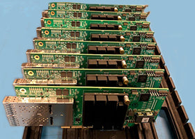
Fred Greenberg started with OSS initially in 2010, and rejoined in 2019. He has been designing products with PCI and PCIe since 1992. He designed one of the first PCIe switch-based single board computers using Gen 1 at 2.5GT/s in 2004. Glenn Rasmuson has been with OSS since 2020, and has done numerous PCIe products starting with PCIe Gen 1. In 2010, he designed a large-scale PCIe Switch Fabric, including multiple switch layers using Gen3. Fred and Glenn designed and delivered OSS’ first PCIe Gen 5 products earlier this year, including a host bus interface card (OSS-PCIe5-HIB732-x16 (579)) and two switched backplanes (OSS-PCIe5-4UP (581 & 580)). The first of these products shipped to a customer in June – an industry first for this class of products.
 |
From an engineering perspective, what have you found is the biggest difference in designing for PCIe Gen 5 vs. PCIe Gen 4? |
| Fred: | Because of the doubling of speed with PCIe Gen 5, the PCI SIG made significant changes in the specification around spacing requirements for signal traces. These changes are deemed necessary to prevent cross talk effects. Cross talk is when the signaling on one trace impacts the signaling on adjacent traces. At higher signaling rates, the probability of cross talk is higher. These requirement changes in the Gen 5 specification cascade through the entire design schematic and layout process. |
| Glenn: | As Fred mentioned, the main change effecting design difficulty was focusing on minimizing cross talk and following new PCI SIG specification, PCIe requirements for system card slots (backplanes), and add-in cards (adapter cards). |
|
What has been the biggest challenge(s)? |
| Fred: | Meeting some of the new requirements for the Gen5 physical layer are not trivial, and are difficult to achieve in terms of signal clearances and clearance to other copper poured areas. We are constrained to the size of boards we want to create, so getting everything to fit in these constraints while ensuring a high level of signal integrity, low noise, and limited cross talk is challenging. Fortunately, the work done by our Gen5 switch vendor, as far as quality of the physical layer and the signals it produces is very good. This has made our work turn out better than expected, in terms of signal integrity. |
| Glenn: | The Broadcom switch’s SERDES is very good, which made it relatively easy to get Gen 5 speeds with good signal integrity across the PCB (printed circuit boards), through connectors and across cables. The SERDES is the physical layer Serializer-Deserializer that is implemented in the PCIe switches. It creates a signal with sufficient margin, which tolerates the losses that will naturally occur as the signal is transmitted throughout the system. However, even with this good signal starting point, the layout of the traces on the board is still a challenge. At Gen5, the need for trace length matching within transmit and receive pairs of a lane is critical, with much higher sensitivity than earlier generations. Without good trace matching in length and signal flight time, you will introduce noise in the signal, which can disrupt signal integrity and introduce errors. |
|
How have you addressed that challenge(s)? |
| Fred: | With these challenges, board layout tends to take longer to meet all the requirements, and we are perfecting these new layout techniques with each new Gen5 design. The layout process is a collaboration between the design engineer and the layout engineer. We have great resources who are highly experienced, including Kermit, who has done some amazing work. Often trace length matching and smooth curves to avoid signal reflections require manual fine tuning, and working beyond what the tools are capable of doing automatically. |
| Glenn: | We focus heavily on PCB route checking. Cross talk and noise are highly impacted by trace routing, and we spend a lot of time insuring we are lowering the risk that we will run into problems. We want to catch and correct any potential issue prior to releasing and creating our first physical samples. |
|
Any particular challenges when thinking about AI Transportable/Edge products? |
| Fred: | If space requirements are factored into the layout, these constraints make our layout task even more difficult. Many AI Transportable solutions are naturally space-constrained, and it is a challenge to both meet these constraints and remain in layout tolerances that naturally want to spread traces out. We often need to make compromises in one dimension or the other. Having a lot of experience in these types of designs helps us know where to make the appropriate trade-offs. |
|
You refer to signal integrity. How do you define that, and why is it important? |
| Glenn: | Signal integrity is the quality of the signal over time, as it moves through the various mediums of a digital system. This includes the PCB (printed circuit board), slot connectors, and if going outside the system, cables as well. With good signal integrity, the information embedded in the signal is easy to discern at its final destination. All of these mediums introduce some level of loss in the quality or amplitude of the signal. These losses accumulate in the transit process, degrading the signal. Once the signal quality drops below a certain level, you can no longer be certain the system is interpreting the intended signal correctly. With Gen 5, this signal needs to be of high quality, while transitioning 32 billion times each second. |
|
In layman’s terms, what is the significance of an ‘eye’ diagram? |

Gen 5 Eye Diagram |
|
| Fred: | The eye diagram is a graphical representation of signal integrity to verify that the signal quality meets requirements for Gen5, as well as other lower speeds where the amplitude (height) and width (time scale) meet and exceed the minimums for a given speed. |
| Glenn: | You can think of it as an image of many bits switching, all superimposed on each other for a given SERDES, that shows how much voltage height and time width margin you have. Diagram 1 is an example of an eye diagram which is measuring the signal on a single PCIe lane. The larger and cleaner the white area, the better the signal integrity. This diagram is an actual measurement of our PCIe Gen 5 products, and is actually very good. |
|
How do you decide what PCB materials to use for PCIe Gen 5? – what are the considerations? |
| Fred: | As the speeds have increased with each generation of PCIe, the importance of the PCB material selection has increased. This is driven by the need to have better, very low loss material. As explained earlier, signal loss needs to be reduced as much as possible, and at Gen 5, the PCB material is critical. The loss of a material is dependent on its material properties and manufacturing process. The less loss, generally the more expensive the PCB. |
| Glenn: | In addition to the material of the PCB, the appropriate stack up design is important. Generally you can think of PCBs being made up of a set of layers that alternate signal layers with ground layers. Tuning the ‘stack-up’ of the PCB is critical for PCIe performance, and for reliable power delivery. In Gen 5, the tolerances for interconnections between signal planes and ground planes are much tighter, and add additional complexity to the design process. |
|
Are there challenges with the tools used to design and debug Gen 5 designs? |
| Fred: | Yes, of course it is not easy to evaluate how well the design is working without being able to see the signals. Avoiding adverse effects by attaching probes of external test equipment is very important. We rely on built-in tools, which are built into our switches. These tools allow us to construct eye diagrams and run signal integrity tests without physically attaching probes. |
Fred and Glenn are part of a talented OSS engineering team, including electric, mechanical, system and software engineers that are delivering state-of-the-art products, uniquely positioned to address the requirements of the fast-growing AI Transportable market.
Click the buttons below to share this blog post!
Comments will be approved before showing up.


Get the latest news, product releases, upcoming events, blog posts and more!